Cadence Circuit Diagram
How to change the wire colour in cadence Cadence circuit schematic for the medradio lna with integrated output Sram cadence 6t conventional
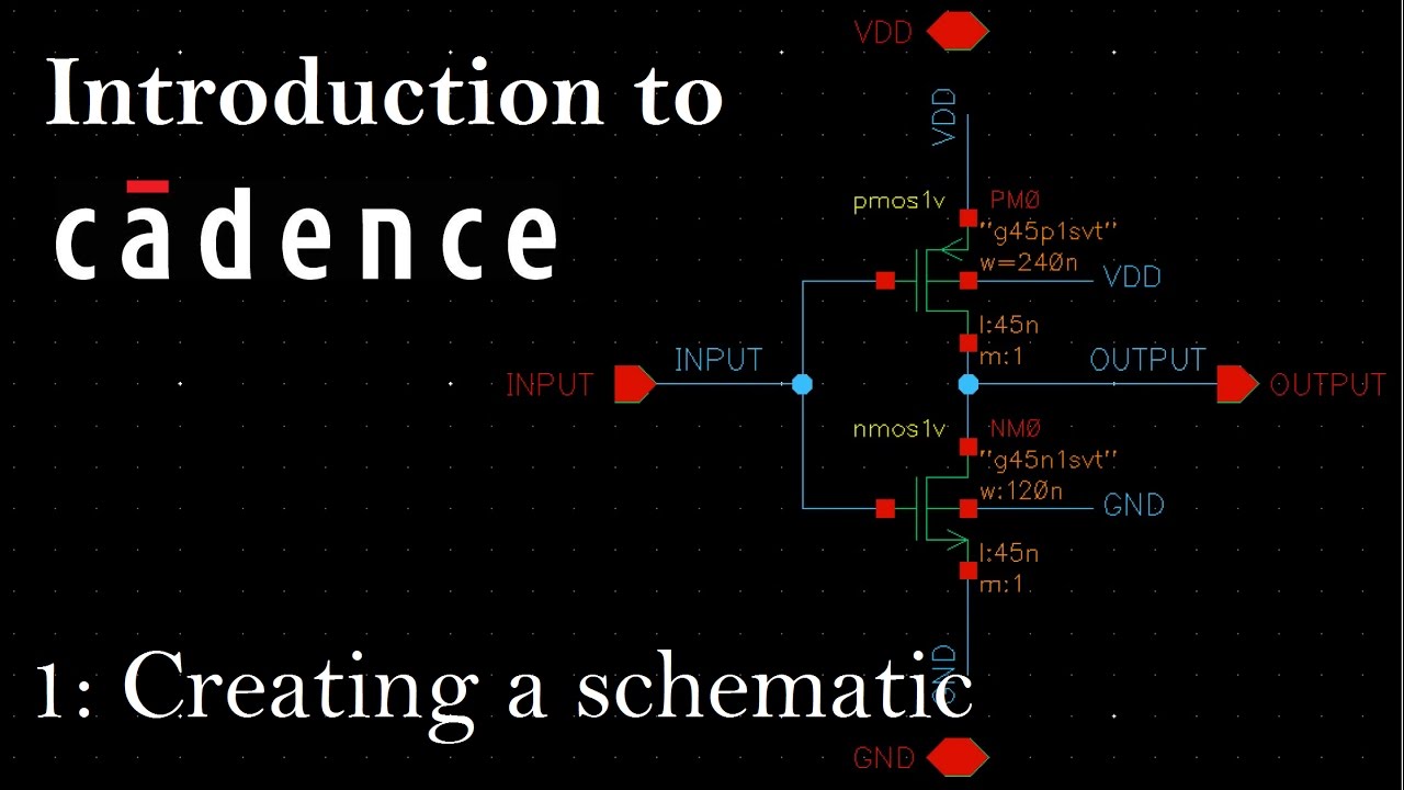
Intro to Cadence 1: Creating a Schematic and Symbol - YouTube
Cadence circuit simulations (the basics) Conventional 6t sram cell design in cadence. Cadence flip flop flipflop
Emojis cadence circuit unicode
Creating schematics in cadenceCadence circuit spectre proposed simulations output Design and implementation of 4-bit flash adc using folding technique inCircuit schematic in cadence design suite.
Virtuoso ic cadence rf semiconductor analog cracker crackDesigner’s guide community :: forum Cadence wire virtuoso change wires colour color defaultIntegrated circuit layout design function.
Cadence schematic symbol virtuoso
Comparator cadence hysteresis cmos circuit schematic internal representation schematics they output understandable maybe clear both same second different justAdc cadence implementation Inverter cadence 65nm simulations virtuosoCadence schematic digitally.
Design of a cmos comparator with hysteresis in cadenceCircuit layout board orcad cadence altium pads printed basic Via technologyDiagram phy ddr ddr5 training lpddr block memory ip cadence modes performance age boosting intro courtesy used.

Cadence circuit
Boosting memory performance in the age of ddr5: an intro to ddrCadence reference bandgap simulation bgr voltage ptat Design vlsi layout and schematic on cadence by ex_einstien_palCadence lna.
Vlsi cadence layout schematic fiverr screenCadence virtuoso – schematic & simulations – inverter (65nm) Nand gate cadence virtuoso input vlsi simulation invertersIntro to cadence 1: creating a schematic and symbol.

Ee4321-vlsi circuits : cadence' virtuoso ultrasim vector file simulation
Cadence compiler integration peakviewDesign of bandgap voltage reference (bgr) A variable digital controlled current source in cadenceCadence® and custom compiler™ integration – lorentz solution.
Cadence mics schematics creating add transform instance appear window will chipLayout of proposed detff all simulations are performed on cadence .


Via Technology - Printed Circuit Board Design and Layout (Cadence

Boosting Memory Performance in the Age of DDR5: An Intro to DDR

Design and implementation of 4-bit flash ADC using folding technique in

Cadence Circuit Simulations (the basics) - YouTube

Design of a CMOS Comparator with Hysteresis in Cadence - MisCircuitos.com

How to change the wire colour in Cadence - MisCircuitos.com

Cadence® and Custom Compiler™ Integration – Lorentz Solution

Integrated Circuit Layout Design Function